Precision in every industry
WiCKON high-tech AOI industry solutions: modular 3D inspection for the highest requirements
WiCKON Hightech offers industrial quality control for high-tech industries, supporting six key sectors with tailored 2D/3D inspection solutions – inline, in the lab, and perfectly integrated into Industry 4.0 environments. Thanks to modular systems, proprietary optics/lighting, and WiSion software, we deliver maximum detection accuracy, real-time feedback, and complete traceability.
Our AOI offers for all industries:
- Inline systems (SPEEDCube, macCube, µInspect)
- 3D inspection heads
- WiSion software & API integration (SECS/GEM, OPC UA)
- Laboratory systems (PerSpectrial)
- Special applications & customized machines
Electronics industry
WiCKON Hightech offers 2D/3D AOI for solder paste inspection (SPI), foils/flexible materials, substrates and end-of-line inspection – ideal for PCB production, power electronics and hybrid assemblies. SPI systems scan typical areas of approx.
3D inspection heads
telecentric optics 1.25-12.5 µm lateral
Combined 2D/3D capture in one scan
WiSion & API
Real-time evaluation
SECS/GEM & OPC UA connection for end-to-end traceability
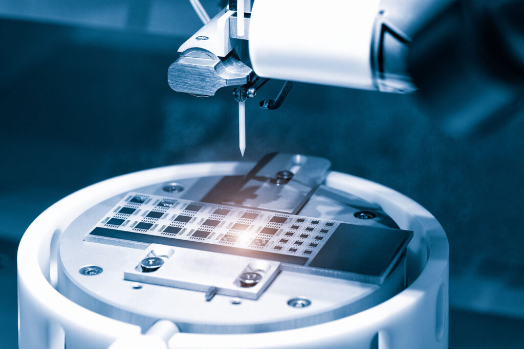
Semiconductor industry
For paste printing on wafers, ceramic/hybrid substrates, wafer topography and wire bonds, WiCKON delivers high-tech metrological precision at high throughputs. Line scan cameras up to 16 384 px at 40-50 k lines/s capture the finest deviations; paste inspections achieve ≤ 0.6 s per 130 × 110 mm section; wire bonds from 13-320 µm are inspected with ± 3.2 µm (1σ) height repeatability.
Inline systems
with closed-loop control (printer/placer – depending on customer setup) and modular resolution/speed
WiSion & API
(SECS/GEM, OPC UA, possibly REST hooks) for fab integration & MES data flows
Medical technology
The focus is on safety and documentation: WiCKON inspects solder pastes, foils/catheter layers, substrates/materials, wire bonds and end-of-line – with 100% coverage and real-time reporting. Telecentric optics (1.25-12.5 µm) and multi-wavelength illumination detect the finest surface and thickness variations; wire bonds are measured with ± 3.2 µm (1σ) repeat accuracy – ideal for implants and sensitive medical electronics.
Aerospace
Aerospace modules require “zero defect”: 3D SPI detects volume deviations, voids and bridges; material/substrate inspection uncovers anomalies in composites and ceramics; EOL inspections ensure complete documentation; wire bond analysis checks the entire bond path and geometries – with ± 3.2 µm (1σ) height repeatability.
Inspection heads
with multi-wavelength illumination and combined 2D/3D acquisition in a single pass
Military technology
Ruggedized AOI for MIL-spec electronics: 3D SPI for solder deposition, EOL inspection of fully populated assemblies, wire bond metrology with ± 3.2 µm (1σ). Real-time reports ensure batch traceability – even under demanding environmental conditions.
Energy sector
From fuel cell pastes (wet & sintered) to solar wafer metallization and ceramic/thick film components: WiCKON Hightech delivers high-throughput inline AOI with 5 µm lateral resolution (solar), full wafer scan ~1.25 s, layer heights 5-30 µm and 10 nm vertical precision for ceramic inspections. Lines with up to 60 substrates/min. are supported.
Are you interested in our hardware, software or services? Do you need industrial quality control for high-tech industries? Are you interested in a product presentation? Write to us – we look forward to hearing from you!